
10th IEEE INTERNATIONAL TEST CONFERENCE INDIA
2026
JULY 19-21, 2026 | RADISSON BLU, MARATHAHALLI, BENGALURU
TUTORIALS
Squeezing Quality into Cents: DFT Strategies for Low-Cost MCUs

Vishal Diwan
Texas Instruments
Vishal Diwan is a Digital Design Manager and Member Group Technical Staff at Texas Instruments, where he leads the DFT team for the ASM Business Unit. With over 13 years of experience in Design-for-Test methodologies, he has developed deep expertise across scan architectures, test automation, and advanced DFT implementation strategies for semiconductor products. He holds a Master's degree in Electrical Engineering from IIT Bombay and has contributed extensively to the field through multiple patents, technical publications, and presentations at industry conferences.
His experience in developing efficient DFT solutions for cost-sensitive, high-volume semiconductor products has given him valuable insight into the trade-offs between test quality, silicon area, test time, and manufacturing cost. This practical perspective enables him to provide a comprehensive view of how innovative DFT methodologies can help deliver reliable MCUs while meeting the aggressive cost targets demanded by today's semiconductor industry.
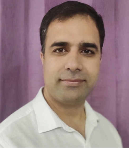
Mudasir Kawoosa
Texas Instruments
Mudasir Kawoosa is a DFT Architect at Texas Instruments (India) Pvt. Ltd. in Bangalore, with fifteen years of industry experience. As a Senior Member of Technical Staff, he leads the centralized DFT team in Connectivity Business Unit driving transformative changes through innovative test solutions, expert silicon bring-up and widely adopted methodologies. Mudasir has architected DFT and test solutions for over fifteen complex System-on-Chip (SoC) programs. He holds master’s degree in electrical engineering from the Indian Institute of Technology, Madras, has published in several peer reviewed external conferences (and is also prolific in TI internal and other conferences), and holds eleven granted US patents. Through his work, he has established several innovative solutions in DFT, test and silicon debug, for a wide variety of chip architectures across several business units in TI, and continues to influence the EDA DFT roadmap.
Low-cost microcontrollers form the backbone of today's connected world, powering applications across IoT, automotive, industrial, and consumer markets. However, delivering high-quality, reliable MCUs at massive production volumes requires balancing stringent cost targets with demanding quality and safety requirements. This tutorial explores Design-for-Test strategies specifically tailored for cost-sensitive MCU designs, addressing challenges such as minimizing silicon overhead, reducing test time, optimizing ATE utilization, managing test power, and maximizing manufacturing throughput. Through practical examples and real-world methodologies, attendees will gain valuable insights into achieving high test coverage and low DPPM while operating within the tight area, power, and cost constraints that define modern MCU development.
LLM for VLSI Design, Automation and Test

Dr. Chandan Karfa
IIT Guwahati
Dr. Chandan Karfa is an Associate Professor in the Department of Computer Science and Engineering at IIT Guwahati, where his research spans electronic design automation, formal verification, hardware security, high-level synthesis, and formal methods. Prior to joining academia, he spent five years as a Senior R&D Engineer at Synopsys, gaining valuable industry experience in semiconductor design automation. A prolific researcher, he has authored more than eighty publications in leading international journals and conferences and has been recognized with several prestigious honors, including the Google India Research Award, Google Silicon Research Awards, Qualcomm Faculty Award, and multiple innovation and best paper awards.
His unique combination of academic research and industrial experience provides him with deep insight into both the challenges and opportunities facing modern semiconductor design flows. Through his work at the intersection of EDA, formal methods, and AI-driven automation, Dr. Karfa brings a forward-looking perspective on how LLMs can transform VLSI design, verification, and test while enhancing the productivity of the next generation of semiconductor engineers.
The growing complexity of modern semiconductor systems is placing unprecedented demands on design, verification, and test workflows. As chips scale to billions of transistors and increasingly heterogeneous architectures, traditional EDA methodologies require significant manual effort and domain expertise to meet aggressive performance, power, and time-to-market targets. This tutorial explores how Large Language Models (LLMs) are emerging as powerful assistants for VLSI engineers, enabling higher levels of automation across RTL design, verification, synthesis, debugging, and test generation. Rather than replacing conventional EDA flows, the session examines how LLMs can augment engineering productivity, streamline development cycles, and redefine the way designers, verification engineers, and test professionals interact with semiconductor design tools in the AI era.
Mission Mode Scan Dump Using IJTAG and TAP Customization: Architecture, Implementation, and Practical Considerations

Sreekanth G Pai
Marvell
Sreekanth G Pai is a Senior Principal Engineer with extensive experience in Design-for-Test, scan architectures, IJTAG infrastructures, and post-silicon debug methodologies for complex SoCs. Throughout his career, he has led and contributed to multiple large-scale silicon programs, developing expertise in TAP customization, mission-mode debug techniques, and Tessent-based DFT implementations.
His work in enabling robust observability, debuggability, and secure access mechanisms across advanced validation and test environments has provided him with deep insight into the challenges of modern post-silicon debug. This experience makes him well positioned to discuss scalable IJTAG-based approaches for mission-mode scan dump and advanced debug architectures.

Raseena K A
Marvell
Raseena K A is a Senior Engineer specializing in DFT implementation, scan architectures, and post-silicon debug for complex SoCs. Her experience includes the development of IJTAG-based infrastructures, scan dump enablement, clock and OCC interactions, and customized debug solutions tailored to mission-mode applications.
Through her work on silicon bring-up and debug using advanced scan and test methodologies, she has developed strong expertise in practical debug execution and validation workflows. Her hands-on experience provides valuable perspectives on implementing efficient, scalable, and reliable scan dump solutions for modern semiconductor systems.
As modern SoCs continue to grow in scale and complexity, effective post-silicon debug has become a critical challenge for ensuring rapid issue resolution and successful product deployment. Traditional test infrastructures often lack the observability required during mission-mode operation, creating the need for more flexible and scalable debug methodologies. This tutorial explores the use of IEEE 1687 (IJTAG) and TAP customization to enable mission-mode scan dump capabilities, providing efficient access to internal silicon states with minimal design impact. Attendees will gain insights into IJTAG-based architectures, scan data extraction techniques, implementation challenges, verification strategies, and practical considerations for enhancing observability and debuggability in advanced semiconductor designs.
Testing Chiplet-Based 2.5D/3D ICs : An Academia/Industry perspective
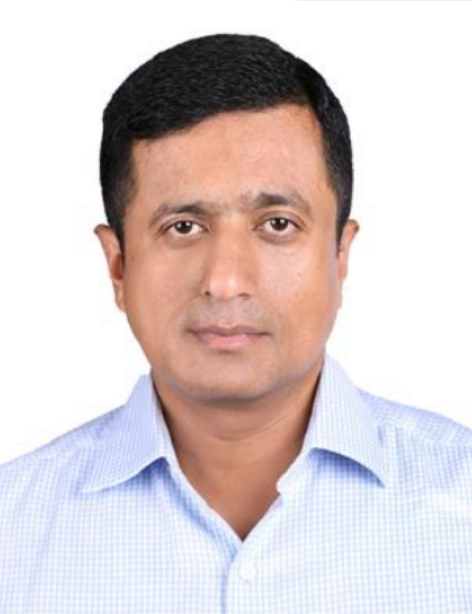
Jyotirmoy Saikia
Cadence
Jyotirmoy is a Software Architect in the Modus DFT R&D group at Cadence Design Systems, where he leads the development of iJTAG, 3DIC Test, and Hierarchical Test technologies. With over 22 years of experience spanning both Electronic Design Automation (EDA) and semiconductor design, he has developed deep expertise in advanced Design-for-Test methodologies. He is a co-inventor of nine U.S. patents and holds an M.Tech. in Computer Science and Engineering from IIT Kanpur.
His extensive work in developing next-generation DFT solutions for advanced semiconductor technologies has given him valuable insight into the evolving challenges of hierarchical testing, chiplet-based architectures, and 3D integrated circuits. By driving innovation in test automation and design enablement, Jyotirmoy continues to contribute to the advancement of scalable and reliable semiconductor test methodologies.

Sagar Kumar
Cadence
Sagar is a Principal Product Engineer in the Modus DFT Software Solutions group at Cadence Design Systems, where he has spent over eight years developing advanced Design-for-Test technologies. His expertise spans iJTAG, Hierarchical Test, Boundary Scan Verification, and 3DIC test methodologies, contributing to the advancement of modern semiconductor test solutions. He holds two patents and earned his M.Tech. in VLSI Systems from VIT Vellore.
Through his work on next-generation DFT technologies and test automation solutions, Sagar has developed strong expertise in addressing the challenges of complex semiconductor architectures. His experience in iJTAG, hierarchical testing, and 3DIC enables him to provide practical insights into scalable and efficient test methodologies for advanced integrated circuits.

Dr. Binod Kumar
IIT Jodhpur
Dr. Binod Kumar is an Assistant Professor in the Department of Electrical Engineering at the Indian Institute of Technology Jodhpur. He received his Ph.D. and M.Tech. in Electrical Engineering from IIT Bombay and his Bachelor's degree in Electronics and Communication Engineering from NIT Silchar. Prior to joining academia, he spent nearly two years at Qualcomm India, where he worked on SoC Design-for-Test, debug, and post-silicon validation strategy development. His contributions to teaching and research have been recognized with the IIT Jodhpur Distinguished Teacher Award (2024) and the Qualcomm Faculty Award (2024).
Drawing on both industrial and academic experience, Dr. Kumar's work focuses on Design-for-Test, validation, and debug methodologies for modern semiconductor systems. His research bridges theoretical advancements with practical implementation, enabling him to provide valuable insights into next-generation DFT and post-silicon validation techniques.

Dr. Jaynarayan T. Tudu
IIT Tirupati
Dr. Jaynarayan T. Tudu is an Assistant Professor in the Department of Computer Science and Engineering at the Indian Institute of Technology Tirupati. He received his Ph.D. from the Indian Institute of Science (IISc), Bangalore, and his research focuses on power-aware computer architecture, Digital VLSI test and verification, and reliable, energy-efficient computing hardware. His work spans Design-for-Testability (DfT), low-power testing, post-silicon debug and diagnosis, fault-tolerant design, and CAD tools for next-generation AI hardware.
Through his research on dependable and energy-efficient semiconductor systems, Dr. Tudu has developed deep expertise in addressing the reliability and testing challenges of modern VLSI and AI accelerator platforms. His work bridges advanced DFT methodologies with emerging computing architectures, offering valuable perspectives on building robust, high-performance hardware from edge devices to data-center-scale processors.
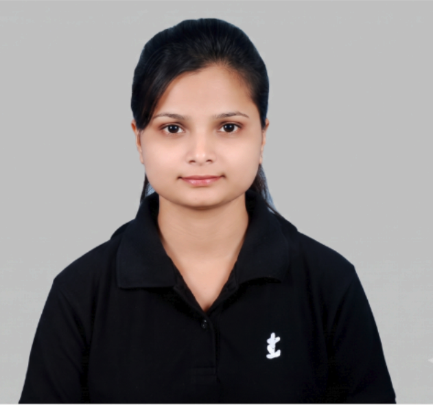
Manisha Kumari
IIT Jodhpur
Manisha Kumari is a Ph.D. Scholar in the Department of Electrical Engineering at the Indian Institute of Technology Jodhpur. Her research focuses on the intersection of VLSI Testing and Electronic Design Automation (EDA), with particular emphasis on 3D chiplet testing and Through-Glass Via (TGV)-based interconnect testing. Her broader interests include semiconductor test, reliability, and the challenges associated with heterogeneous integration and advanced 3D packaging technologies.
Through her research on next-generation testing methodologies for advanced packaging and chiplet-based systems, Manisha is contributing to solutions for the evolving reliability and test challenges of modern VLSI designs. Her work provides valuable insights into emerging test strategies that will support future heterogeneous and three-dimensional semiconductor architectures.
The semiconductor industry is rapidly transitioning from monolithic System-on-Chip (SoC) designs to 2.5D and 3D multi-die architectures to meet the growing demands for higher performance, improved power efficiency, greater scalability, and faster time-to-market. While these advanced integration technologies offer significant system-level advantages, they also introduce unprecedented test and reliability challenges arising from heterogeneous integration, limited access to buried dies, complex die-to-die interconnects, and compounded yield loss across multiple stacked components. This tutorial provides a comprehensive overview of the testing methodologies for 2.5D and 3D integrated systems, covering the complete test flow from pre-bond and mid-bond testing to post-bond and system-level validation. Participants will learn about scalable Design-for-Test (DfT) architectures and standardized test access mechanisms that enable efficient delivery of test data through stacked dies while ensuring thorough validation of both individual dies and high-density die-to-die interconnects. Further, the tutorial also presents emerging AI-assisted testing methodologies for three-dimensional chiplet integration using micro-bump interconnects, where interface densities can reach thousands of connections per die. AI-based approaches for different types of interconnect defect detection and fault localization will be introduced, demonstrating how machine learning can significantly improve test quality and diagnostic accuracy for complex multi-die systems. Finally, the tutorial explores one of the latest advances in advanced packaging—glass substrate-based 2.5D/3D chiplet System-in-Package (SiP) technology. It discusses the unique testing challenges associated with Through Glass Vias (TGVs) and presents effective test strategies for ensuring the reliability and manufacturability of next-generation glass-based packages. Attendees will gain a practical understanding of state-of-the-art testing techniques, emerging AI-driven test solutions, and future trends that are shaping the test ecosystem for advanced 2.5D and 3D chiplet-based semiconductor systems.
Closed Loop Test Engineering – From Design to Mass Production
Maheedhar Jalasutram
Maheedhar Jalasutram leads DFT Architecture within Google's Silicon team, where he is responsible for developing scalable test architectures that balance quality, coverage, and test cost for advanced mobile SoCs. Throughout his career, including leadership roles at Google and Texas Instruments, he has driven innovations in concurrent testing, design-for-debug, high-speed test methodologies, and system-level test enablement.
His extensive experience spanning DFT architecture, validation, and production test has provided him with deep insight into the challenges of delivering high-quality silicon at scale. This expertise enables him to offer a unique perspective on how test methodologies can be integrated across the entire product lifecycle to improve both quality and manufacturing efficiency.
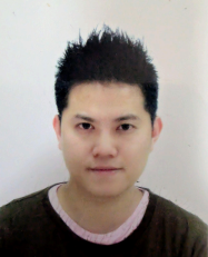
Jeren Ku
Jeren Ku leads the Foundry, Assembly Process, and Yield Engineering team within Google's Custom Silicon Operations organization. He oversees manufacturing operations, yield improvement, process optimization, quality management, and product ramp activities for Google's custom silicon programs. Prior to Google, he held leadership positions at Intel and TSMC, focusing on advanced semiconductor process technologies, including FinFET and Gate-All-Around transistor development.
His experience across process technology development, manufacturing operations, and yield engineering has given him a comprehensive understanding of how design, fabrication, and production data interact to influence product quality. This background provides valuable insight into building closed-loop methodologies that accelerate yield learning and production readiness.

Daejin Shin
Daejin Shin leads the Product Engineering and Quality team within Google's Custom Silicon Operations organization, overseeing test yield analysis, manufacturing operations, supply chain quality, and OSAT engagement for multiple generations of Google silicon products. His team plays a key role in delivering scalable, high-quality semiconductor solutions while driving operational excellence across the manufacturing ecosystem.
Through his work at the intersection of product engineering, quality management, and high-volume manufacturing, he has developed deep expertise in leveraging test and yield data to improve product robustness and production efficiency. His experience provides valuable perspectives on establishing effective feedback loops between design, test, and manufacturing to achieve world-class quality outcomes.
As semiconductor products become increasingly complex and quality expectations continue to rise, achieving ultra-low DPPM while maintaining aggressive cost targets requires tighter integration between design, test, and manufacturing. This tutorial explores the concept of Closed Loop Test Engineering, demonstrating how Design-for-Test and Volume Product Engineering can work together to optimize product quality, yield, and test efficiency throughout the silicon lifecycle. Covering topics such as advanced DFT architectures, fault coverage strategies, yield analysis, test optimization, diagnosis methodologies, and production feedback mechanisms, the session provides a comprehensive framework for connecting design decisions with manufacturing outcomes to drive continuous improvement from silicon development through mass production.
Machine Learning is Inevitable or Not: A DFT Designer’s View
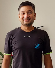
Ankush Srivastava
Qualcomm
Ankush Srivastava is a semiconductor test expert with over 19 years of industry experience and currently leads the development of advanced Design-for-Test methodologies for Qualcomm's cutting-edge SoCs. Holding a doctorate from IIT Bombay and a degree from BITS Pilani, he has made significant contributions to semiconductor test technology through numerous patents, technical publications, intellectual property developments, and presentations at leading international conferences.
His extensive work in DFT automation, test optimization, and next-generation validation methodologies has given him deep insight into the evolving intersection of machine learning and semiconductor testing. As an active contributor to the global test community through organizations such as ITC, ATS, VLSI Design, and VDAT, Ankush brings a practical and forward-looking perspective on how AI can be effectively leveraged to improve DFT productivity, test quality, and silicon success.
Artificial Intelligence and Machine Learning are rapidly transforming engineering workflows across the semiconductor industry, creating both new opportunities and new challenges for Design-for-Test (DFT) engineers. As modern SoCs continue to increase in complexity, traditional DFT methodologies face growing demands for faster turnaround times, improved test quality, lower power consumption, and reduced defective-parts-per-million (DPPM). This tutorial explores the practical application of machine learning in DFT, covering areas such as ATPG optimization, test point insertion, test coverage enhancement, IR-drop analysis, and intelligent DFT automation. It also examines the emerging role of AI-driven assistants and large language models in streamlining DFT workflows, while providing a balanced perspective on where machine learning can deliver meaningful value—and where engineering expertise remains indispensable.
Beyond Scan Dump: Why IEEE P2929 Enables True Scan State Extraction
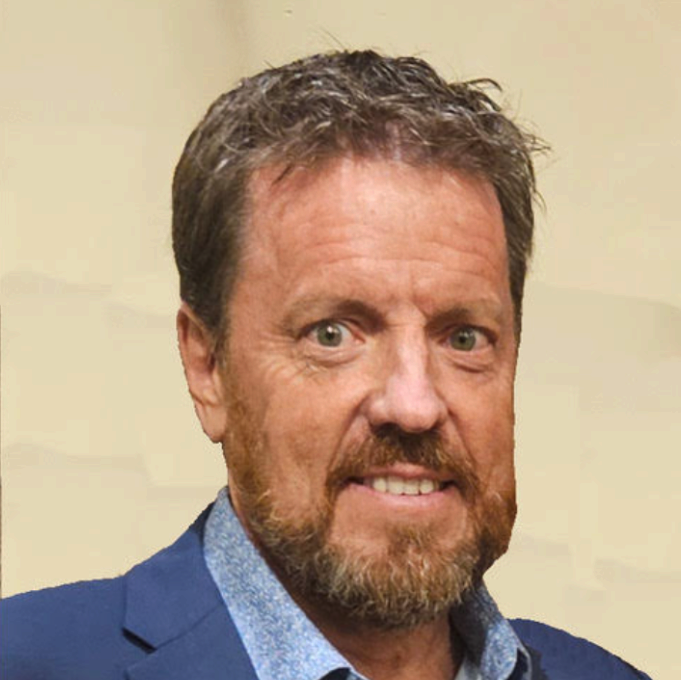
Andy Hughes
Siemens EDA
Principal Product Engineer specializing in new technologies utilizing Tessent Streaming Scan Network. Andy has over 25 years’ experience in DFT related product development, 10 years in direct chip design and a MS in Comp Eng from USC. He recently joined the Tessent family in 2025 after 20 years at Cadence Design Systems and has been instrumental in bringing the Scan State Extraction product to market. Andy is currently a member of the IEEE P2929 working group that is driving the Scan/Array Debug Standards.
This tutorial, will cover the details on the new and emerging IEEE P2929 standard and the technology that refines the process of doing a raw dump of scan data into an optimized accurate full functional post-silicon debug Scan state extraction
Testing to Self Testing: Self Test Driven Functional Safety for ISO 26262 Compliant Automotive SoCs

Rajesh Kumar Tiwari
Qualcomm India
Rajesh Kumar Tiwari is Director of Engineering at Qualcomm India, with over 22 years of experience in semiconductor design and Design-for-Test technologies. Over the course of his career at Qualcomm and Texas Instruments, he has led the development of advanced DFT architectures, in-system BIST solutions, and test methodologies across mobile, compute, and automotive platforms. He is also an active contributor to the semiconductor test community through his involvement with IEEE initiatives and technical innovations.
His extensive experience in deploying self-test and safety-focused DFT solutions for complex SoCs has given him deep insight into the challenges of achieving functional safety in modern automotive systems. This expertise positions him uniquely to discuss the evolving role of self-test technologies in enabling ISO 26262-compliant semiconductor designs.

Mohammed Zuber P Malek
Qualcomm India
Mohammed Zuber P Malek is a Senior Staff Engineer and Manager at Qualcomm India with more than 17 years of experience in Design-for-Testability. Having contributed to over twenty successful chip tape-outs, he has developed extensive expertise across in-system BIST, scan synthesis, ATPG, low-power testing, TestSTA, and RTL-level DFT integration. He currently leads Qualcomm's Auto-DFT methodology and TestSTA initiatives, driving scalable and robust test solutions for advanced SoC programs.
His work in architecting automated DFT methodologies and self-test infrastructures for complex silicon platforms has provided him with valuable insight into the intersection of functional safety, diagnostics, and test automation. This experience enables him to offer practical perspectives on leveraging self-test technologies to meet the reliability and compliance requirements of next-generation automotive systems.
As automotive systems evolve into software-defined, safety-critical computing platforms, ensuring functional safety throughout a vehicle's lifecycle has become a fundamental requirement. Traditional manufacturing and validation testing alone are no longer sufficient to meet the stringent demands of ISO 26262 compliance. This tutorial explores how Built-In Self-Test (BIST) technologies are transforming functional safety architectures by enabling continuous in-field fault detection, diagnostics, and reliability monitoring. Covering logic BIST, memory BIST, mission-mode testing, and safety-driven test strategies, the session provides practical insights into designing scalable, standards-compliant automotive SoCs capable of delivering robust safety assurance from silicon to system.
The Seamless Integration of Packetized Scan and In-System Test with Advanced ATE Equipment

Hagen Goller
Advantest
Hagen started his work career in 1997 and moved into Semiconductor Test in 2001. Since then, he has held various positions in Application Support, Marketing and R&D around the Advantest V93k ATE Platform. Currently he is a technical director in product marketing, looking into new test methodologies and solutions for both ATE and SLT.
As semiconductor devices continue to increase in complexity, reducing test cost while maintaining high quality and reliability has become a key industry challenge. Emerging technologies such as packetized scan architectures and in-system test methodologies are transforming how structural tests are delivered, enabling more efficient use of Automatic Test Equipment (ATE), reducing test data volume, and extending test capabilities beyond manufacturing into system-level and in-field environments. This tutorial provides an overview of packetized ATPG data generation, configuration, and deployment, highlighting how seamless integration with advanced ATE platforms supports scalable test delivery, enhanced diagnostics, data logging, and long-term product reliability throughout the silicon lifecycle.
Advanced Test Data Analytics for Yield and Quality Improvement

Shamitha Rao
Synopsys, India
Shamitha Rao is Director of Solutions Engineering at Synopsys, where she leads customer engagements for the TestMAX product portfolio. With more than 20 years of experience spanning DFT architecture, implementation, silicon validation, and test solutions, she has held key roles at Synopsys, Intel, Siemens EDA, STMicroelectronics, and Wipro. Her contributions to semiconductor test technology have been recognized through multiple technical publications, conference presentations, and industry awards.
Her extensive experience across the semiconductor lifecycle—from design and test architecture to silicon bring-up and manufacturing—provides her with a unique perspective on how advanced analytics can be leveraged to improve product quality, yield learning, and test efficiency in modern semiconductor ecosystems.

Shrestha Hota
Synopsys
Shrestha Hota is a Staff Solutions Engineer at Synopsys with over a decade of experience in semiconductor manufacturing analytics and yield engineering. She specializes in architecting analytics frameworks that enable yield optimization, root-cause analysis, and operational efficiency across high-volume manufacturing environments. Her work focuses on deploying advanced analytics platforms that transform complex manufacturing data into actionable insights.
Through her leadership in customer engagements and data-driven manufacturing initiatives, she has developed deep expertise in applying analytics to solve real-world semiconductor production challenges. This experience positions her at the forefront of modern yield engineering and intelligent manufacturing solutions.

Navya Rastogi
Synopsys
Navya Rastogi is a Staff Applications Engineer at Synopsys with expertise spanning semiconductor process engineering, yield analysis, fabrication technologies, and data science. Prior to joining Synopsys, she gained experience in both the semiconductor capital equipment industry and at Amazon, bringing a multidisciplinary perspective to advanced manufacturing analytics. She holds a PhD in Nanoscience from the Indian Institute of Science.
Her background across semiconductor processes, yield engineering, and data-driven problem solving provides her with valuable insight into the application of analytics for improving manufacturing performance and product quality in advanced semiconductor technologies.
As semiconductor technologies continue to scale and heterogeneous integration becomes increasingly prevalent, the volume and complexity of test and manufacturing data have grown exponentially. Extracting actionable insights from this data has become essential for accelerating yield ramp, improving product quality, reducing scrap, and enhancing manufacturing efficiency. This tutorial explores modern data analytics methodologies within the Silicon Lifecycle Management (SLM) framework, covering advanced statistical techniques, machine learning applications, root-cause analysis, yield monitoring, and real-time quality management. Attendees will gain practical insights into leveraging both local and cloud-based analytics platforms to transform vast semiconductor test datasets into data-driven decisions that improve yield, reliability, and operational excellence.
Understanding Test Escapes and the Limitations of Scan DFT Testing
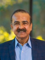
Adit D. Singh
Auburn University
Adit D. Singh is the Godbold Endowed Chair in Electrical and Computer Engineering at Auburn University and a globally recognized authority in VLSI test, reliability, and semiconductor quality. Over a distinguished academic and research career spanning more than four decades, he has made pioneering contributions to defect-based testing, adaptive testing, and statistical methods for integrated circuit validation. A Life Fellow of IEEE, he has authored more than 300 technical publications, holds internationally licensed patents, and has served in numerous leadership roles across the global semiconductor test community.
His extensive research, industry collaborations, and deep involvement in advancing test methodologies have provided him with unparalleled insight into the challenges of test escapes and timing-related failures in modern semiconductor devices. Combining rigorous academic research with practical industry perspectives, he brings a uniquely authoritative view on improving test effectiveness and ensuring reliable operation of increasingly complex integrated circuits.
As semiconductor devices continue to scale in complexity and performance, test escapes have emerged as a critical challenge impacting product quality and system reliability. Despite advances in scan-based testing, cell-aware methodologies, and system-level test strategies, timing-related defects continue to evade detection, leading to operational failures and, in some cases, silent data corruption in large-scale computing environments. This tutorial provides a comprehensive examination of the root causes behind test escapes, the limitations of existing scan and system-level test methodologies, and the effectiveness of emerging timing-aware test approaches. Drawing on industrial production data and recent research, the session offers valuable insights into improving defect detection, enhancing test quality, and addressing the growing reliability challenges associated with advanced semiconductor technologies.
Scalable ATE Hardware Design: From Concept to Manufacturing with Reusable Architecture

Lokapriya Balakrishnan
Caliber Interconnects
Lokapriya Balakrishnan is a Test Engineer at Caliber Interconnects with over seven years of experience in semiconductor testing and ATE interface hardware development. Her work spans turnkey load board and probe card design, signal and power integrity optimization, device testing, and tester platform conversion projects. In addition to her technical contributions, she has successfully led engineering teams in delivering high-quality hardware solutions within demanding development schedules.
Her experience across both hardware development and semiconductor validation provides her with a unique perspective on the challenges of designing scalable, high-performance ATE solutions. This expertise enables her to bridge the gap between hardware architecture, test requirements, and manufacturing realities.
Senthilkumar Dhamodharan
Caliber Interconnects
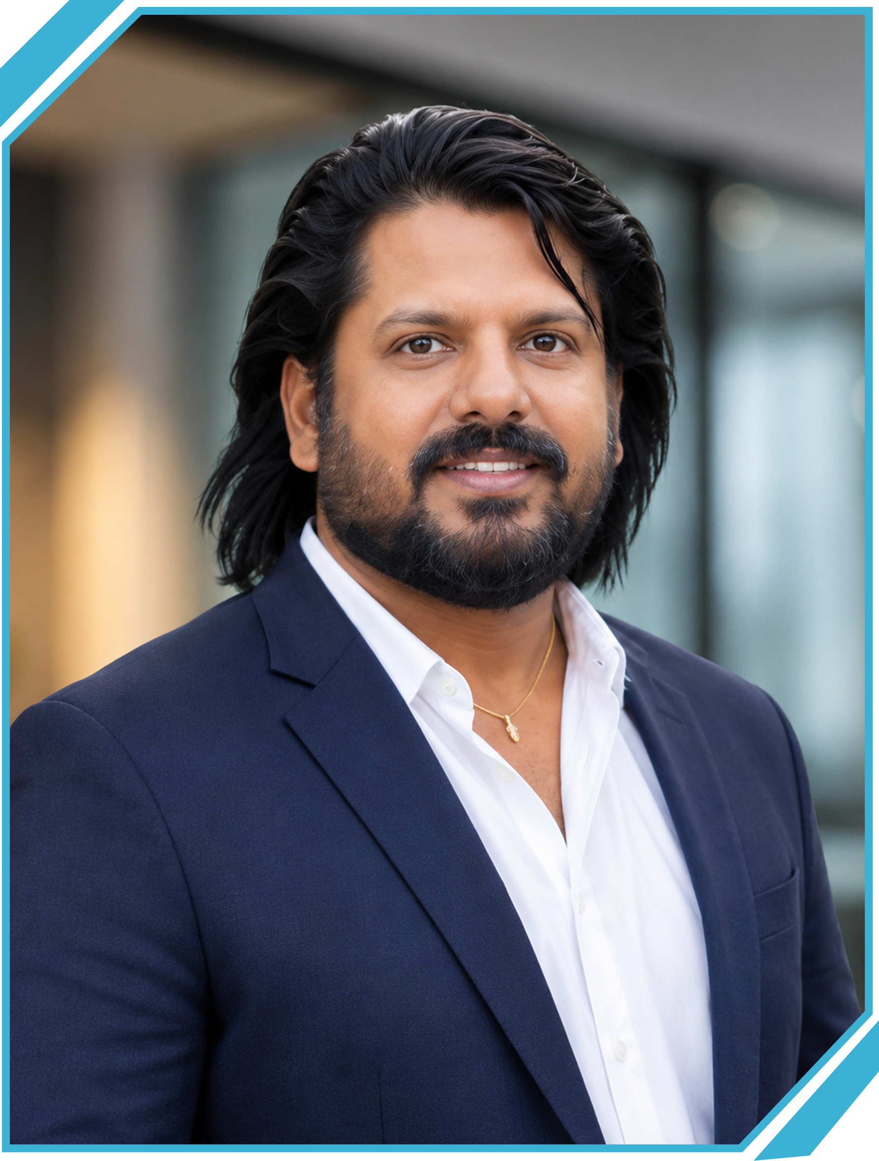
Senthilkumar Dhamodharan is Vice-President of Semiconductor Test Engineering at Caliber, where he leads the Test Engineering Division responsible for validating SoC, PMIC, Digital, Mixed-Signal, and RF products across ATE and bench platforms. With over 19 years of experience at industry leaders including Qualcomm, AMD, and NXP, he has built deep expertise in semiconductor test, physical design, DFT, and high-volume manufacturing. He also drives strategic initiatives in intellectual property development and leads a high-performance engineering organization of more than 250 test engineers. He holds a Master's degree in VLSI Design from Anna University.
Drawing on extensive leadership across semiconductor validation, manufacturing test, and engineering strategy, Senthil has played a pivotal role in advancing innovative test methodologies for complex silicon products. His experience in building scalable engineering organizations and driving next-generation test solutions provides him with valuable insights into the evolving landscape of semiconductor testing and intelligent silicon.

Dyaneswaran Anguraj
Caliber Interconnects
Dyaneswaran Anguraj is currently serving as a Test Engineer at Caliber Interconnect Solutions and possesses over 19 years of diverse experience spanning both academia and the semiconductor industry, with deep expertise in PCB CAM, PCB design, and advanced semiconductor test engineering. He holds a Master’s degree in Applied Electronics and began his career with a focus on PCB design, specializing in layout development, signal integrity, and manufacturing support. He later transitioned into academia, serving as an Assistant Professor at reputed engineering institutions, where he mentored future engineers, led impactful research initiatives, and contributed to peer-reviewed publications. Currently, he works as a Test Engineer at Caliber Interconnects, where he focuses on the validation and characterization of digital, mixed-signal, and memory ICs. He has hands-on experience with leading ATE platforms supporting both engineering debug and high-volume production test development. His responsibilities include designing and executing comprehensive test plans, optimizing test coverage, automating test procedures, and delivering robust and efficient test solutions that meet stringent quality standards and time-to-market requirements.
As semiconductor devices continue to push the boundaries of speed, power, and integration, the complexity of Automated Test Equipment (ATE) hardware design has increased significantly. Achieving reliable signal and power integrity while maintaining scalability, cost efficiency, and rapid deployment is now a critical requirement for successful device validation. This tutorial presents a comprehensive approach to designing robust ATE hardware, covering Device Interface Boards (DIBs), SI/PI methodologies, simulation-driven design practices, manufacturing readiness, and validation workflows. A key focus is the adoption of reusable hardware architectures based on modular motherboard-daughtercard concepts, enabling faster development cycles, improved scalability, and enhanced first-time-right success across diverse semiconductor product families.
Customer Centric Post Silicon Validation Approach for System on Chip (SoC)

Ravishankar Manishankar
Intel
Ravishankar Manishankar is a validation expert at Intel with over 21 years of experience spanning System-on-Chip platform validation, functional validation, and embedded wireless software development. Throughout his career, he has worked extensively in areas including PCIe, CXL, customer platform validation, benchmark enablement, and DSP firmware systems engineering across 2G, 3G, 4G, and DAB technologies. He also brings valuable academic experience from the United States, where he conducted research and taught advanced wireless communication topics.
His extensive background across silicon validation, software development, and customer platform enablement has provided him with a holistic understanding of the challenges involved in bringing complex SoCs to market. This combination of technical depth and real-world deployment experience gives him unique insight into customer-centric post-silicon validation methodologies and the tools, processes, and strategies required to ensure successful silicon qualification and deployment.

Siloni Palani
Intel
Siloni Palani is a validation engineer at Intel with over nine years of experience in pre-silicon and post-silicon validation for data center GPUs and complex SoCs. Her expertise spans concurrency testing, platform validation, LPDDR5 memory systems, validation tool development, and automation frameworks. She has played a key role in hardware bring-up activities and system-level validation efforts focused on enhancing product quality and debug efficiency.
Through her work on complex silicon platforms, validation infrastructure, and automation-driven workflows, she has developed deep expertise in identifying, diagnosing, and resolving system-level issues throughout the product lifecycle. Her experience provides valuable perspectives on modern validation practices and the importance of scalable, customer-focused approaches to post-silicon validation in increasingly sophisticated semiconductor systems.
As System-on-Chip (SoC) designs become increasingly complex, ensuring reliable silicon deployment requires a comprehensive validation strategy that extends well beyond fabrication and pre-silicon verification. Post-Silicon Validation (PSV) plays a critical role in bridging the gap between design intent and real-world customer usage, enabling early issue detection, efficient debug, and improved product quality. This tutorial provides a practical overview of customer-centric PSV methodologies, covering silicon bring-up, design-for-debug infrastructure, validation planning, benchmark-driven testing, and unified software frameworks that support both pre- and post-silicon environments. Attendees will gain insights into industry-standard validation flows, debug techniques, and test reuse strategies that accelerate product readiness while improving system reliability and customer experience.