Tutorial Program
| Sunday | 24 July, 2022 | |||
|---|---|---|---|
| 8:30 am - 9:30 am | REGISTRATIONS | ||
| TRACKS | TRACK 1 | TRACK 2 | TRACK 3 |
| HALL NAME | HALL - 1 | HALL - 2 | HALL - 3 |
|
9:30 am - 11 am ( 15 mins Break ) 11:15 am - 12:45 pm |
T1: Scan Test Escapes, New Fault Models, and Effectiveness of Functional System Level Tests
Authors: Prof. Adit Singh (Auburn University) |
T2: Basics of Design for Test – Enabling Manufacturing Test
Authors: Sreekanth Pai and Balaji Upputuri (Marvell) |
T3: Hierarchical DFT techniques for AI and Large SoCs
Authors: Lee Harrison (Siemens) |
|
T4: Bridging the Gap Between Design-For-Test and Failure Analysis for Yield and Reliability Improvements
Authors: Rakesh Kinger and Gaurav Mattey (Google) |
T5: Challenges and Advances in Power-Aware Testing
Authors: Ankush Srivastava (Qualcomm) |
||
| 12:45 pm - 1:45 pm | LUNCH BREAK | ||
|
1:45 pm - 3:15 pm ( 15 mins Break ) 3:30 pm - 5:00 pm |
T6: A Complete DFT Methodology from Chip Planning to Implementation
Authors: Niranjani Sukumar and Salvatore Talluto (Synopsys) |
T7: Addressing Test, Safety and Security for Connected Automotive IC’s
Authors: Lee Harrison and Nilanjan Mukherjee (Siemens) |
T8: Challenges of High Accuracy and Low-cost Test for Analog Power ICs, and the future Trends
Authors: Gaurav Mittal (Texas Instruments) |
|
T9: Practical aspects of Implementing IEEE 1687
Authors: Rajesh Khurana and Vivek Chickermane (Cadence), Balaji Upputuri (Marvell) |
|||
| Sunday | 24 July, 2022 | |||
|---|---|---|---|
| 8:00 am - 9:30 am | REGISTRATIONS | ||
| TRACKS |
TRACK 1 Session Chair | Dr. Subhadip Kundu |
TRACK 2 Session Chair | Shamitha Rao |
TRACK 3 Session Chair | Prof. Sivanantham |
| HALL NAME | GRAND VICTORIA - A | GRAND VICTORIA - B | ARABICA & ROBUSTA |
|
9:30 am - 11 am ( 15 mins Break ) 11:15 am - 12:45 pm |
T1: Scan Test Escapes, New Fault Models, and Effectiveness of Functional System Level Tests
Prof. Adit Singh (Auburn University) |
T2: Basics of Design for Test – Enabling Manufacturing Test
Sreekanth Pai and Balaji Upputuri (Marvell) |
T3: Hierarchical DFT techniques for AI and Large SoCs
Lee Harrison (Siemens) |
|
T4: Bridging the Gap Between Design-For-Test and Failure Analysis for Yield and Reliability Improvements
Rakesh Kinger and Gaurav Mattey (Google) |
T5: Challenges and Advances in Power-Aware Testing
Dr. Ankush Srivastava (Qualcomm) |
||
| 12:45 pm - 1:45 pm | LUNCH BREAK | ||
|
1:45 pm - 3:15 pm ( 15 mins Break ) 3:30 pm - 5:00 pm |
T6: A Complete DFT Methodology from Chip Planning to Implementation
Niranjani Sukumar and Salvatore Talluto (Synopsys) |
T7: Addressing Test, Safety and Security for Connected Automotive IC’s
Lee Harrison and Dr. Nilanjan Mukherjee (Siemens) |
T8: Challenges of High Accuracy and Low-cost Test for Analog Power ICs, and the future Trends
Gaurav Mittal (Texas Instruments) |
|
T9: Practical aspects of Implementing IEEE 1687
Rajesh Khurana and Dr. Vivek Chickermane (Cadence), Balaji Upputuri (Marvell) |
|||
Tutorial 1
Title: “Scan Test Escapes, New Fault Models, and the Effectiveness of Functional System Level Tests“
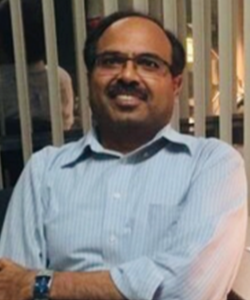
Speaker: Prof. Adit D. Singh (Auburn University)
Prof. Adit D. Singh (Auburn University)
Bio:
Adit Singh is James B. Davis Professor of Electrical and Computer Engineering at Auburn University, where he has served on the faculty since 1991. Earlier he has held faculty positions at the University of Massachusetts in Amherst, and Virginia Tech, in Blacksburg; and visiting professorships at the University of Freiburg, Germany, and the University of Tokyo, Japan. His research interests span all aspects of VLSI technology. He is particularly recognized for his pioneering contributions to statistical methods in test and adaptive testing. Dr. Singh has held leadership roles as General Chair/Co-Chair/Program Chair for dozens of VLSI design and test conferences and continues to serve on the Steering and Program Committees of many major international conferences in test and design automation. He served two terms (2007-11) as Chair of the IEEE Test Technology Technical Council (TTTC), and (2011-2015) on the Board of Governors of the IEEE Council on Design Automation (CEDA). Dr. Singh holds a B.Tech in Electrical Engineering from IIT Kanpur, and the M.S. and Ph.D. from Virginia Tech. He was elected Fellow of IEEE in 2002.
Abstract:
This tutorial aims at understanding the increasing use of functional system level tests (SLTs) as an additional final defect screen before processor SOCs are shipped for assembly. For this, we take an in-depth look at traditional scan based Stuck-at and TDF tests to understand potential sources of test escapes. We also extensively discuss the effectiveness of new test generation methodologies such as Cell Aware, Gate Exhaustive, Transistor Stuck-Open, and Timing Aware in plugging these structural test holes. Based on this, we identify failures that can still remain undetected by low-cost scan structural tests, and require the use of expensive functional SLTs to achieve desired defect levels. In conclusion, we suggest strategies to minimize use SLTs without impacting defect levels.
Tutorial 2
Title: “Basics of Design for Test – Enabling Manufacturing Test“
Speaker: Sreekanth G Pai and Balaji Upputuri (Marvell)
Sreekanth G Pai (Marvell)
Bio:
Sreekanth G Pai is a Principal Engineer, Design for Test in Central Engineering ASIC BU at Marvell India Pvt Ltd. Sree is currently leading end to end DFT implementation and validation on a customer chip while actively mentoring multiple DFT engineers to achieve DFT Execution Excellence. Sree has been a DFT Engineer for the past 10 years. His expertise ranges from creating best in class flows for DFT implementation/validation to defining and implementing custom DFT solutions to cater to Customer/Design needs and end to end DFT execution on complex customer designs. He joined Marvell India Pvt Ltd in 2019 through Avera Acquisition. He specializes in Hierarchical Test and Power Aware Testing. He has 2 filed patents along with multiple publications in technical forums such as ITC, VLSI-D, DAC, ISLPED, CDNLive.
Balaji Upputuri (Marvell)
Bio:
Balaji is currently working as Principal Engineer DFT, part of CE ASIC team. He has Joined Marvell in Nov2019 from Avera acquisition. He Has overall 16+ years of industry experience, Started VLSI journey from VEDAIIT Hyderabad after graduation in Electronics and communications from JNTU Hyderabad. He has started career with verification, FPGA and moved to DFT domain. Balaji has a wide set of expertise in DFT ranging from IP DFT, DFT implementation, PreSi Validation to Post-si debug. Currently, Balaji is focusing on defining DFT architecture solution for a 7nm and a 5nm complex network ASIC chips. He is adept at defining custom DFT solutions and his focus is to ensure First time right hardware. He holds 6 patents and 20 publications all of which are meaningful and relevant Innovations. Each of these ideas is highly impactful in improving Quality of Results and Turn Around time for DFT/Test solutions.
Abstract:
This tutorial is intended to cover basic topics in DFT.
A list of topics that we plan to cover are as given below
- An introduction to Manufacturing Test
- Yield, DPPM, Faults, Fault Models (10 mins)
- Introduction to Fault Models
- Basics of Scan based Testing
- Introduction to Scan Compression
- Introduction to ATPG Flow
- Simulations (with and without Timing annotation)
- Diagnosis (5 mins)
Tutorial 3
Title: “Hierarchical DFT techniques for AI and Large SoCs“
Speaker: Lee Harrison (Siemens)
Lee Harrison (Siemens)
Bio:
Lee Harrison is Automotive IC Test Solutions Manager, with Mentor, A Siemens Business. He has over 20 years of industry experience with Mentor DFT products and has been involved in the specification of new test features and methodologies for Mentor customers, delivering high quality DFT solutions. With a focus on Automotive, Lee is working to ensure that current and future DFT requirements of Mentor’s automotive customers are understood and met. Lee Received his BEng in MicroElectronic Engineering from Brunel University London in 1996.
Abstract:
The era of artificial intelligence (AI) and large chip designs has come. Cloud and infrastructure applications in AI are booming with new design architectures, methodology, technologies and design-for-test (DFT) requirements. CPU, GPU, FPGA, ASIC, DSP and many other technologies are used in large chips, which lead to many new architectures. We found it is very important for us to understand these new architectures and new technologies from both design and DFT point of view. This tutorial will cover the DFT challenges how a a range of technologies and a hierarchical approach can address these challenges.
Tutorial 4
Title: “Bridging the Gap Between Design-For-Test and Failure Analysis for Yield and Reliability Improvements“
Speaker: Rakesh Kinger and Gaurav Mattey (Google)
Rakesh Kinger (Google)
Bio:
Rakesh Kinger is currently responsible for DFT Productization tasks for consumer products silicon in Devices and Services (DSPA) group at Google. Rakesh has more than 25 years of hands-on experience in various areas related to Design-for-Test (DFT) implementation, silicon and system level test and debug, test quality, reliability and manufacturing. Before joining Google, Rakesh was responsible for leading DFT activities for complex network switching chips at Broadcom and for mobile SOCs at Qualcomm. Rakesh is the co-inventor for three US issued patents and has published multiple papers in international test and failure analysis related conferences. His areas of interest include Mixed Signal IPs testing, At-speed testing of SOCs, Memory and Logic
Gaurav Mattey (Google)
Bio:
Since graduating with his Master’s degree in Electrical Engineering-Solid State Electronics from the University of Michigan, Gaurav has 10+ years of experience in the Semiconductor industry specializing in Failure Analysis, Quality & Reliability, Yield bring-up, Scan/ATPG/MBIST Diagnosis, ATE based Test Engineering & Semiconductor Process Technology. Gaurav’s role currently at Google Devices and Services (DSPA) group is that of NPI development Test Engineering Lead, responsible for ATE Test bring-up, Failure Analysis and DFT Diagnostics flow. Prior to joining Google, Gaurav worked as a Technical Lead for Microprocessor Product Development Engineering focusing on Failure Analysis & Yield bring-up for Mobile SOCs at Qualcomm and Graphics, Desktop and Server products at Advanced Micro Devices (AMD). Gaurav has published papers at international conferences and is also the co-author of a US issued patent in the fields of Test & Failure Analysis.
Abstract:
Design for Testability (DFT) diagnosis and Failure Analysis (FA) play a very important role in identifying the key bottlenecks, especially during first silicon bring up in a new technology node. Effective diagnosis for both memory and logic defects help in identifying critical test, design marginality and process issues in a timely and efficient manner. However, as the process technology continues to scale and with increased design complexity, numerous challenges arise during FA. This tutorial covers the topic of bridging this gap between DFT implementation, diagnosis and FA so that some of these challenges can be met to ensure a very high success rate of identifying the defects. This tutorial will discuss different memory and logic defect diagnosis techniques along with any special requirements for DFT hardware and associated test modes and test patterns needed for facilitating FA. These techniques will be very instrumental in identifying critical criteria for FA candidate selection like the suspects/symptoms count, diagnostics score, physical proximity of suspects in layout, etc that would produce a high success rate. Electrical Fault Isolation (EFI) technique is selected depending on the type of failing pattern (Structural v/s Functional) and the parametric dependence (if any) of the failure across different voltage, frequency, temperature, etc. For advanced design debug on Automatic Test Equipment (ATE) and System Level Test (SLT) platforms, there are other sophisticated techniques used like Dynamic Laser Stimulation, Photon/Thermal Emission and Laser Voltage Probing/Imaging. Each of these techniques has its distinct test patterns and looping methodology requirements for compatibility with the associated FA tool. Such test-patterns need to be developed through close partnership with the DFT team. This tutorial will cover the details of such special test time optimized test patterns requirements like compression logic bypass, 1-hot chain patterns, PLL based trigger, etc. that enables EFI for FA. High quality and accurate fault isolation data drives downstream tools for physical FA (like nano-probing & TEM) that help to visualize the defects and/or identify process and design marginalities for feedback to foundry & yield learning. This effort will also help to dramatically reduce the number of costly physical failure analysis to identify systematic defects.
Tutorial 5
Title: “Challenges and Advances in Power-Aware Testing“
Speaker: Dr. Ankush Srivastava (Qualcomm)
Dr. Ankush Srivastava (Qualcomm)
Bio:
Ankush Srivastava is currently involved in enabling DFT methodologies for Qualcomm’s state-of-the-art SoCs. He Has 15 years of industrial experience – Freescale/NXP/Qualcomm . He holds several international patents, journals and presented various papers in premier IEEE conferences. His current research interests include defining DFT architecture of complex SoCs, system security related to debug interfaces, effective and efficient small-delay defect-oriented test generation and low-power test methodology. He did his Ph.D. from IIT Bombay and M.E. from the BITS Pilani, all in Electrical Engineering. His Hometown is Lucknow and cycling is his hobby.
Abstract:
The tutorial aims at understanding the issues of over-testing due to power supply droop during at-speed scan testing. The tutorial will start with the problem definitions and most recent solutions being offered either from the hardware designers or using CAD centric solutions. It will be proceeded by the pre-silicon and post-silicon hot-spot analysis with their respective effectiveness. At the end, we suggest effective strategies to minimize parametric yield loss due to over testing and possible efficient solutions available today.
Tutorial 6
Title: “A Complete DFT Methodology from Chip Planning to Implementation“
Speaker: Niranjani Sukumar, Adam Cron, Salvatore Talluto, Rahul Singhal, Harish K Prabhakar (Synopsys)
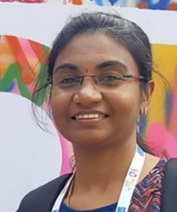
Niranjani Sukumar (Synopsys)
Bio:
Niranjani Sukumar is a Solutions Manager at Synopsys in Hardware Analytics and Test group. Her current focus is on development of RTL based reference flows and reference methodologies. She had lead various methodology initiatives for gate level Scan flows. Niranjani received her MS (Micro Electronics) from Manipal University and BE (Electrical and Electronics) from Amrita Institute of Technology and Science.
Adam Cron (Synopsys)
Bio:
Adam Cron is a Distinguished Architect at Synopsys working with customers worldwide on complex Security, DFT, and ATPG issues for SoCs. He is part of the Hardware Analytics and Test R&D group, and has been with Synopsys for over 24 years. Adam is helping to automate the implementation of secure silicon as part of the DARPA AISS program. Adam is Chair of IEEE Std 1838 which standardized 3D-IC test access, editor of IEEE Std P1149.4, and is an IEEE Golden Core recipient. He also chairs a working group creating a Rest API for MITRE’s CWE and CAPEC databases.

Salvatore Talluto (Synopsys)
Bio:
Salvatore Talluto started in 1987 as an Asic Designer in Alenia Avionic Systems (currently Leonardo), he is now a DFT and Automation Architect in Synopsys, where he joined in 1998, supporting and developing DFT methodologies for major European customers, with focus on Automotive.
Rahul Singhal (Synopsys)
Bio:
Rahul Singhal is a Product Manager for TestMAX DFT at Synopsys. His focus is the industry requirements and solutions in the areas of test compression, ATPG, and DFT for AI architectures. He developed and presented tutorial on DFT for AI chips and has co-authored multiple papers, posters on DFT and test in leading IEEE conferences. Rahul received his MS in Electrical Engineering from Portland State University and BS in Electrical Engineering from Purdue University.
Harish K Prabhakar (Synopsys)
Bio:
Harish K Prabhakar is a Senior Staff Solutions Engineer at Synopsys. He began his career at Wipro and worked for Mindtree, Qualcomm & MediaTek before joining Synopsys. He has around 14 years of experience in VLSI industry working on Design for Testability (DFT). He has worked extensively on DFT implementation on multiple SoCs. Harish’s current focus is on implementing Turnkey projects for customers spread across different geographies. He leads a team of engineers working on all fields of DFT. Harish has a Bachelor’s degree in Electronics and Communication from Nehru College of Engineering & Research Centre under Calicut University
Abstract:
Growing demands of chips across multiple product segments and wide variety of complex architectures not only introduce challenges in chip design while it brings more challenges to Test. The challenges in DFT are seen across various disciplines such as clocking, power, performance, area, safety, security, reliability, in-system testing and so on. In this tutorial we introduce DFT implementation at RTL level with its benefits along with incremental low level synthesis-based DFT and cover the complete flow right from chip planning to implementation. We discuss the flow overview including planning and steps involved in taking care of various disciplines for DFT implementation and validation prior to DFT, during DFT and post DFT.
Tutorial 7
Title: “Addressing Test, Safety and Security for Connected Automotive IC’s “
Speaker: Lee Harrison and Nilanjan Mukherjee (Siemens)
Lee Harrison (Siemens)
Bio:
Lee Harrison is Automotive IC Test Solutions Manager, with Mentor, A Siemens Business. He has over 20 years of industry experience with Mentor DFT products and has been involved in the specification of new test features and methodologies for Mentor customers, delivering high quality DFT solutions. With a focus on Automotive, Lee is working to ensure that current and future DFT requirements of Mentor’s automotive customers are understood and met. Lee Received his BEng in MicroElectronic Engineering from Brunel University London in 1996.
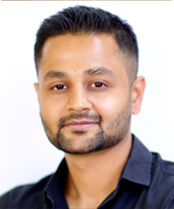
Nilanjan Mukherjee (Siemens)
Bio:
Nilanjan Mukherjee is a Senior Director of Engineering for Tessent Silicon Lifecyle Solutions at Siemens EDA. He has been actively involved in the R&D of key technologies in the areas of test quality, test compression, Logic BIST, Memory BIST, low power DFT, and diagnosis. Some of his major accomplishments include being a co-inventor and an architect of EDT/TestKompress, the VersaPoint Test Points technology, a Low Power Hybrid EDT/Logic BIST scheme for automotive ICs, and the Observation Scan Technology (LBIST-OST). Currently, his focus is on developing new test solutions for automotive and data-center markets.
Nilanjan has co-authored more than 85 technical papers and is a co-inventor of 55 US patents. He has received numerous awards including Best Paper Awards at VTS 2020, VLSI Design 2009, ATS 2001, and VTS 1995, the Most Significant Paper Award at ITC 2012, Siemens DISW Invention of the year 2019, and the Donald O. Pederson Outstanding Paper Award in 2006.
Nilanjan received a B.Tech. (Hons) degree from IIT, Kharagpur, and a Ph.D. degree from McGill University, Canada. He has given numerous tutorials, short-term courses, and invited talks at premier IEEE/ACM conferences, symposia, universities, and companies across the world.
Abstract:
This tutorial will focus on the expanding requirement and regulations surrounding test, safety and security for Automotive IC’s. Looking at the various technologies and methodologies that can be used to address the different challenges and how these are being integrated to standardize and automate this process. We will deep dive into a wide range of different test and functional safety technologies, with a focus on traditional structural test and safety technologies, to more advanced system level testing IP used to collect operational data from the IC. We will also look at the security implications surrounding these technologies.
Tutorial 8
Title: “Challenges of High Accuracy and Low-cost Test for Analog Power ICs, and the future Trend“
Speaker: Gaurav Mittal (Texas Instruments)
Gaurav Mittal (Texas Instruments)
Bio:
Gaurav has 14 years of industry experience in analog test engineering. He is currently the test manager for Power Switching, Interface and Lighting business units at Texas Instruments, owning more than 5 investment areas for TI. He and his team focus on power protection and distribution devices across all analog market segments including automotive, industrial, PE, communication, and enterprise. He is the test architect for the group driving the test roadmap strategy, identifying the test gaps, and driving the systematic closure for them. Gaurav has a proven track record of self-sustaining test solutions and drove systematic cost, performance, and quality leadership at test, for these cost and quality-sensitive power devices. Since 2008, he has worked and defined test strategies across a variety of power devices including fuses, Hot-swap, LDO, ideal diode, current loop protectors, and high side drivers. Gaurav is a Member Group of Technical Staff (MGTS) at Texas Instruments since 2019. He has 14 papers (external and internal), 1 patent, an industry talk at the Asian test Symposium (ATS2019), and provided course lecture for VLSI test at IISc.
Abstract:
With high levels of integration using semiconductors, integrated circuits used for power monitoring and distribution (aka power ICs) face additional challenges from perspectives of transient protection, power dissipation and efficiency. The ATE production testing of these power ICs needs to deal with the contrarian trends of increasing load currents & accuracy requirements at one end, and shrinking ATE-error budgets & test costs at the other end. Specific test challenges include effective calibration of process-dependent parameters at high currents, reliable probe touchdowns against small pad size constraints, achieving low test costs using standard ATEs, improving measurement inaccuracies against poor thermals and self-heating at high currents, etc. Additionally, the use of such power ICs in automotive systems puts further demands on shipped product quality. The first segment of the tutorial will explain the recent trends in power ICs, roles & features, and these evolving challenges as mentioned above. It will also cover several test innovations to achieve these objectives, namely novel DFT implementations, test hardware solutions, and production test methodologies. The second segment of the tutorial will cover the ATE infrastructural challenges, overview & limitations of existing flows, and industry trends on newer ATE platforms. It will also describe the generic semiconductor manufacturing flow and packaging trends, providing broader perspectives on the challenges shown in the first segment. We shall wrap up the tutorial by discussing the future trends of Analog testing, quality aspects, and cost challenges. We shall also touch upon data analytics trends & adaptive testing on these devices, ATE co-simulation, and outlier detection trends.
Tutorial 9
Title: “Practical aspects of Implementing IEEE 1687“
Speaker: Rajesh Khurana, Dr. Vivek Chickermane (Cadence), Balaji Upputuri (Marvell)
Rajesh Khurana (Cadence)
Bio:
Rajesh is currently working as Director R&D at Cadence Design System, Noida, and leads a team working on IEEE 1687 & Low Power Tests. Prior to joining Cadence, he was Engineering Manager at Synopsis Bangalore office. He has over 25 years of experience spanning across multiple domains & technologies. His current interests are in Low Power Test methodologies and Embedded Macro Tests using IEEE 1687 and 1500. His contribution in the field of research includes five US patents and multiple publications at ITC (both India & US), ATS, NATW etc. He has master’s in management and bachelor’s in electrical engineering from DEI, Dayalbagh Agra.
Dr. Vivek Chickermane (Cadence)
Bio:
Vivek Chickermane is a Distinguished Engineer and a Senior Group Director for R&D in the Modus DFT Software in FED/DSG. Vivek is currently leading the productization of 3D IC DFT and Hierarchical Test and also researching Hardware Security.
Vivek has published more than 90 technical refereed technical articles and papers and is also an inventor/co-inventor of more than 60 US patents. He serves on several IEEE conference and standards committees and is currently an Associate Editor of IEEE Design & Test. He received his B.Tech in Electrical Engineering from Indian Institute of Technology, New Delhi and his M.S and Ph.D degrees in Computer Engineering from the Univ. of Illinois at Urbana-Champaign.
Balaji Upputuri (Marvell)
Bio:
Balaji is currently working as Principal Engineer DFT, part of CE ASIC team. He has Joined Marvell in Nov2019 from Avera acquisition. He Has overall 16+ years of industry experience, Started VLSI journey from VEDAIIT Hyderabad after graduation in Electronics and communications from JNTU Hyderabad. He has started career with verification, FPGA and moved to DFT domain. Balaji has a wide set of expertise in DFT ranging from IP DFT, DFT implementation, PreSi Validation to Post-si debug. Currently, Balaji is focusing on defining DFT architecture solution for a 7nm and a 5nm complex network ASIC chips. He is adept at defining custom DFT solutions and his focus is to ensure First time right hardware. He holds 6 patents and 20 publications all of which are meaningful and relevant Innovations. Each of these ideas is highly impactful in improving Quality of Results and Turn Around time for DFT/Test solutions.
Abstract:
The IEEE 1687 standard has rapidly gained popularity in the industry and is becoming the de facto method to deal with IP handoff and integration. IP developers can use the ICL and PDL files to describe their Instruments/IP blocks and the functional patterns, and these same files can be used by an EDA tool to re-target the functional tests to the SoC boundary. The 1687 standard inherently leverages the 1149.1 TAP interface for select, control and operation of a TDR within an Instrument, and has also found application in configuration of Hierarchal Tests and complex designs with LBIST and MBIST. This is even being used to control the turn/elevate inter-die logic for 3D Tests. This tutorial describes usage and application of 1687 and how it is being used to meet the Test and DFT requirements. It will cover how the IEEE 1687 standard can be used for retargeting of functional tests, configuration of Hierarchal Tests in presence of LBIST and MBIST, 3D Tests and explain the ICL and PDL languages, describe the most important constructs in the standard and how to use them. We will also discuss some of the advanced concepts like iMerge, Broadcast and Hierarchal SIB based designs which do not have sufficient explanation/examples in the standard.
-
The Conference
-
Read Blogs
-
Latest Agenda
-
Keynote
-
Tutorial Program
-
General Inforamtion
-
Committee
-
Contact Us
Event Location
Radisson Blu Hotel, Bengaluru Outer Ring Road
Address: 90/4 Outer Ring Road, Marathahalli, Bengaluru, 560037, India
Google Maps Direction: https://goo.gl/maps/nyvHRWcNstifH6TE6